- HOME
- Topics
- News Release
- 2023
December 12, 2023
Establishes Technologies for EUV Lithography System Pellicles Enabling Formation of Fine Circuits for Next-Generation Semiconductors
LINTEC Group has established technologies for EUV lithography system pellicles, which is indispensable for the formation of fine circuits for next-generation semiconductors.
Dust-proof Material Essential for Formation of Fine Circuits in Next-Generation Semiconductors
As communications systems become more sophisticated and faster, semiconductor circuit patterns are becoming increasingly finer. With the improved performance of the extreme ultraviolet (EUV) lithography systems used to form fine circuits, the development of more durable pellicles becomes vital. Pellicles are components that act as anti-dust membrane to prevent foreign matter from adhering to photo-masks (original plates of circuits). These components, which must be transparent, heat resistant, and durable enough for the EUV used to form circuits as fine as five nanometers (one-billionth of a meter) or less, contribute to greater semiconductor productivity.
While conventional pellicles have been made of polysilicon and other materials, pellicles made of carbon nanotubes (CNTs: tubular carbon molecules) have recently been attracting attention as new, more durable materials have become necessary. The LINTEC Group has been exploring new applications for CNTs for some time at its Nano-Science & Technology Center (NSTC), located in the U.S. state of Texas, which has been working on developing CNT sheets. As part of this focus, the Center began to develop CNT pellicles in 2018 and has now successfully established a higher level of elemental technology.
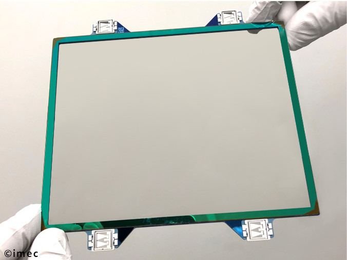
Image of CNT pellicle sheet (photo courtesy of imec)
Supplying Components Made With Proprietary Carbon Nanotube Sheet Technologies
Although CNTs are an extremely thin carbon material with a diameter measuring just nanometers, they are resistant to chemical changes and strength loss even when subject to high temperatures, making them suitable for use in harsh environments. Considering that expectations are high that CNTs will prove useful in a wide variety of applications, the Group will invest approximately five billion yen between now and fiscal 2025 to establish the first CNT mass production system with a particular focus on semiconductor-related applications.
The contents of the News Release are as of the announcement date. Please note that they may differ from the latest information.