February 17, 2026
Latest Developments in CNT Pellicle Technology for EUV Lithography Presented at International Conference
LINTEC has developed a new coating formulation that significantly enhances the durability of CNT (carbon nanotube) pellicles for Extreme Ultraviolet (EUV) lithography.
Through joint research on mass-production technologies with the Semiconductor Frontier Research Center of the National Institute of Advanced Industrial Science and Technology (AIST), LINTEC is promoting research and development aimed at establishing an initial mass-production system for CNT pellicles (clean-conservation materials) essential for forming fine patterns in advanced semiconductors.
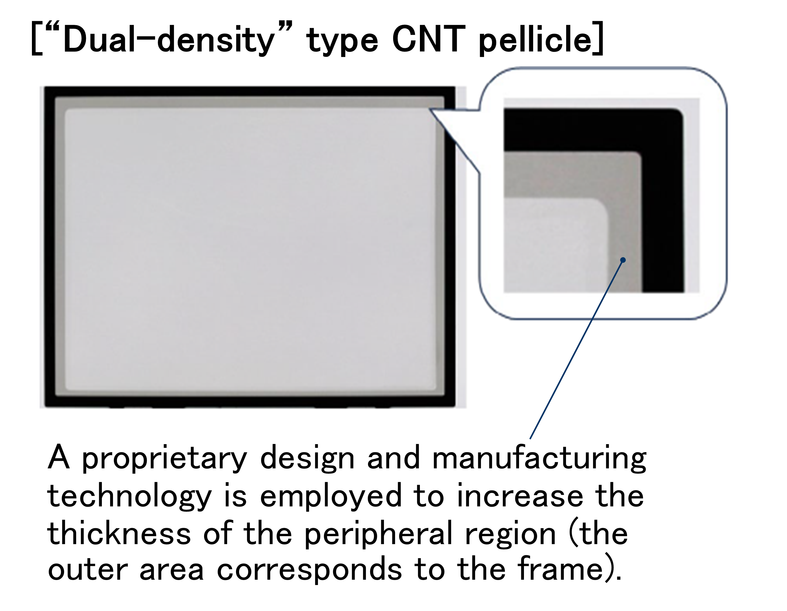
In addition, the company has independently developed a "Dual-density" type CNT pellicle with enhanced durability in EUV exposure environments. This is achieved by increasing the thickness of the pellicle's outer peripheral area. The company has established mass production technology for "Dual-density" type CNT pellicles. Details will be presented this February at SPIE Advanced Lithography + Patterning, an international conference to be held in San Jose, California, USA.
- ・Event Name: SPIE Advanced Lithography + Patterning
- ・Dates: February 22 (Sunday)-26 (Thursday)
- Note. The above technology will be presented on February 25 (Wednesday), 17:30-19:00 in Hall 2 (poster presentation), and on February 26 (Thursday), 8:20-8:40 in Grand Ballroom 220A (oral presentation).
- ・Venue: San Jose Convention Center (San Jose, California, United States)
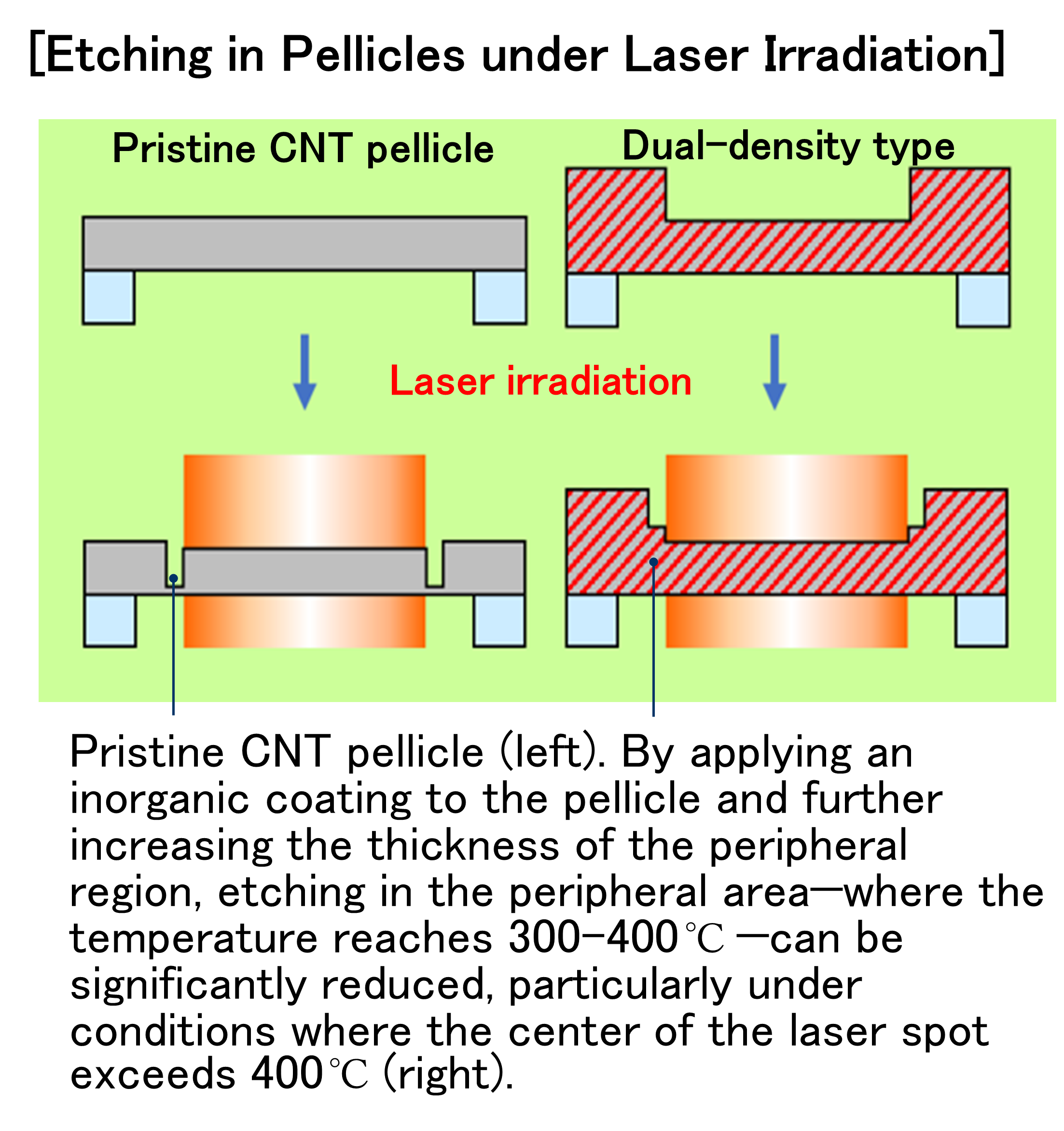
LINTEC analyzed thermal impact data on pellicles under conditions close to those of actual lithography systems using a hydrogen plasma etching system designed in-house. In scanner environments operating in the low-to-medium light source power range, where pellicle temperatures reach 300-400°C, LINTEC established a new inorganic coating formulation that prevents etching in pellicles induced by hydrogen plasma within the system, and confirmed a significant improvement in durability.
Pellicles for EUV Lithography Systems
EUV lithography systems are used for forming fine circuit patterns in advanced semiconductors. As the performance of these systems continues to improve, the development of pellicles with higher durability is increasingly required. A pellicle is a protective membrane that prevents contaminants from adhering to the photomask (the master plate of circuit patterns) and is required to exhibit high EUV permeability as well as excellent heat resistance and durability. Through joint research with the Semiconductor Frontier Research Center of AIST, LINTEC is engaged in the development of CNT pellicles aimed at mass production that meet stringent performance requirements.
"Dual-density" type CNT pellicles
Under laser-induced heating, the etching rate of CNT pellicles caused by hydrogen plasma is known to increase to temperature ranges of approximately 300-400°C. At higher temperatures, however, the etching rate is rapidly suppressed, and it has been confirmed that etching scarcely progresses at temperatures above 900°C.
Based on this temperature dependence characteristics of CNT pellicles, LINTEC has been developing various coating formulations to suppress etching in pellicles. Anticipating that future increases in EUV light source output may cause the peripheral regions of pellicles to reach temperature ranges where etching is more likely to occur, LINTEC has independently developed a "Dual-density" type CNT pellicle with increased thickness at the peripheral region to enhance durability.
About the National Institute of Advanced Industrial Science and Technology (AIST)
The National Institute of Advanced Industrial Science and Technology (AIST), one of the largest public research organizations in Japan, focuses on the creation and practical realization of technologies useful to Japanese industry and society, and on "bridging" the gap between innovative technological seeds and commercialization.
For this, AIST is organized into 5 departments and 2 centers that bring together core technologies to exert its comprehensive strength.
AIST, as a core and pioneering existence of the national innovation system, has about 2300 researchers doing research and development at 12 research bases across the country, based on the national strategies formulated bearing in mind the changing environment regarding innovation.
- >>Website AIST: About AIST
Semiconductor Frontier Research Center (SFRC)
The "Semiconductor and Digital Industry Strategy" (released in June 2021 and revised in June 2023) by the Ministry of Economy, Trade and Industry (METI) clearly states the policy to secure the semiconductor manufacturing base in our country and to promote the establishment of next-generation technologies and R&D for future technologies. AIST has been formulating the "Next Generation Computing Infrastructure Strategy" (June 2022) and has been conducting research and development to realize the goals of the strategy. Semiconductor Frontier Research Center (SFRC) aims to accelerate these activities and ensure advanced semiconductor technology in Japan. The SFRC also aims to become a Center of Excellence (COE) for promoting open innovation in advanced semiconductors through consistent implementation of research and development, construction of shared pilot lines, social implementation, and human resource development.
The contents of the News Release are as of the announcement date. Please note that they may differ from the latest information.