- HOME
- Topics
- News Release
- 2024
September 26, 2024
Accelerating Advanced EUV Lithography Pellicle Mass Production by Joint Research with AIST on Nanolithography Component Technologies
LINTEC Group has been pursuing joint research with the National Institute of Advanced Industrial Science and Technology (AIST) since October 2023 to establish its first high-volume manufacturing (HVM) system for the next-generation extreme ultraviolet (EUV) lithography pellicle, a fine particle filter for high numerical-aperture (NA) EUV lithography essential for nanometer-size circuitry production of advanced semiconductors. LINTEC is pleased to announce that the research progress achieved to date paves the way for implementing HVM processes and will be accelerating its efforts to operate HVM systems by the end of 2025.
Steady Progress on Mass Production Development
EUV lithography system is used to manufacture highly advanced semiconductors, which requires a sophisticated pellicle to filter out tiny particles, preventing them from adhering to photomasks, the blueprints of fine circuitry in semiconductor products. The pellicle for next-generation lithography systems must meet ever stringent criteria, such as higher transparency, stronger heat resistance, and long lifetime, to be compatible with EUV and high NA-EUV lithography and to boost semiconductor productivity.
With the steadily growing moment of manufacturing advanced semiconductor equipment and materials in Japan, LINTEC's R&D Center in Texas, USA, which focuses on carbon nanotube (CNT) film research, developed highly competitive CNT pellicles with its prototype production system in 2023. Under its joint research with AIST pursuing mass production technologies, LINTEC created its HVM system equipment in July 2024. This achievement, stemming from the joint efforts, marks the opening of a new era of next-generation EUV pellicle manufacturing.

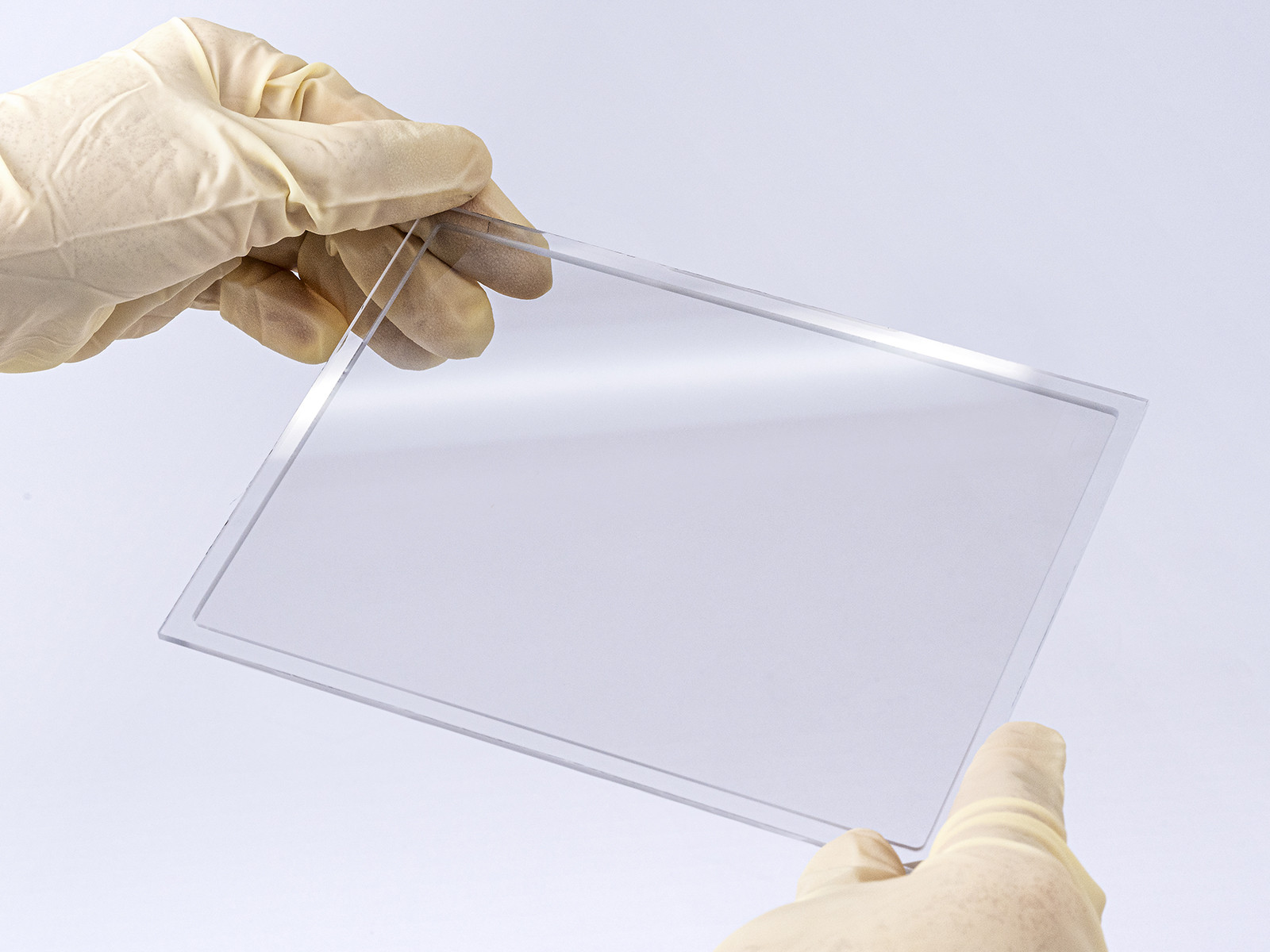
CNT-based pellicle membrane

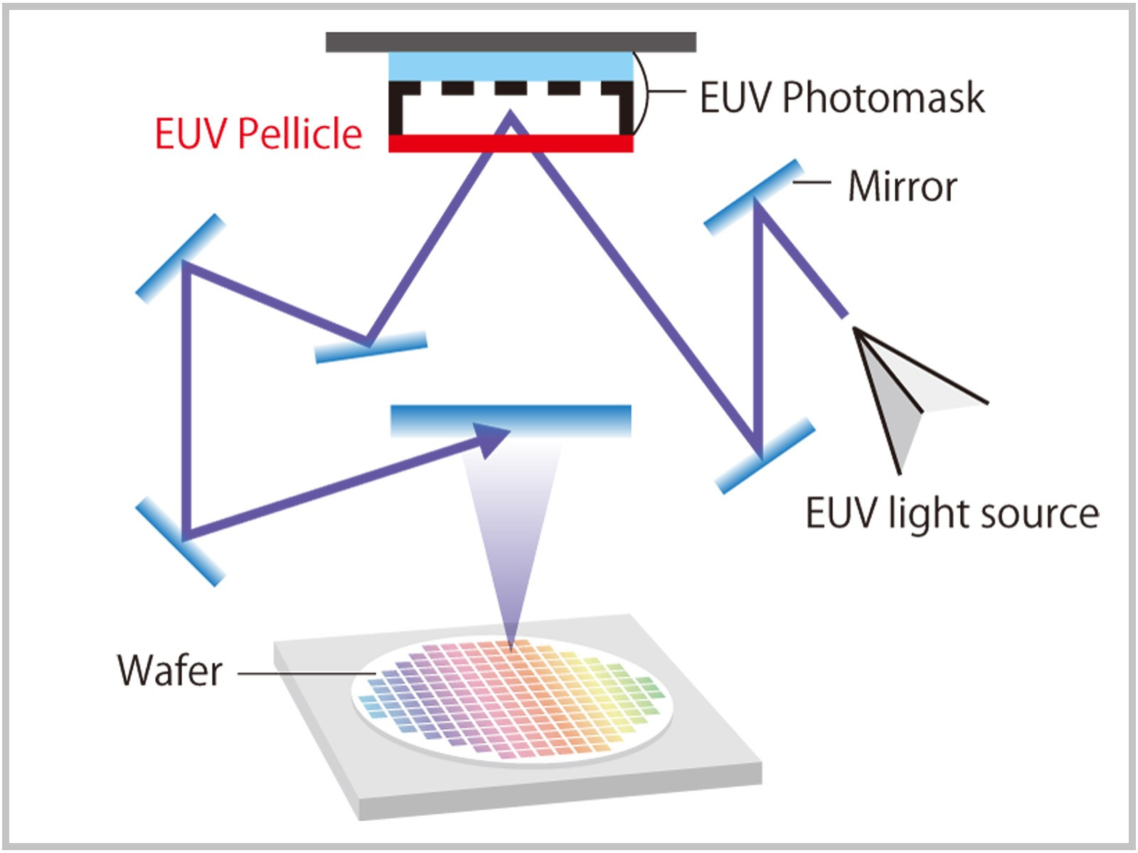
Illustration of EUV lithography system interior
Consolidation of R&D Results and Upscaling Production for Semiconductor Industry
Alongside the joint research with AIST on fundamental nanolithography technologies* for next-generation semiconductor device manufacture, LINTEC's R&D Centers in Saitama-shi, Saitama Prefecture, Japan, and in Texas, U.S.A., have been advancing the development of necessary pellicle and pellicle production technologies, aiming to establish HVM systems for CNT-based pellicles. In addition, Ina Technology Center, another LINTEC development site in Kitaadachi-gun, Saitama Prefecture, is developing its own pellicle mass production equipment. This group additionally focuses on developing pellicle characterization and quality assurance equipment, including EUV transmittance measuring devices. LITNEC is consolidating these results to establish HVM systems and EUV pellicle mass productions by the end of FY2025 to facilitate high-NA EUV pellicle implementation in the semiconductor industry.

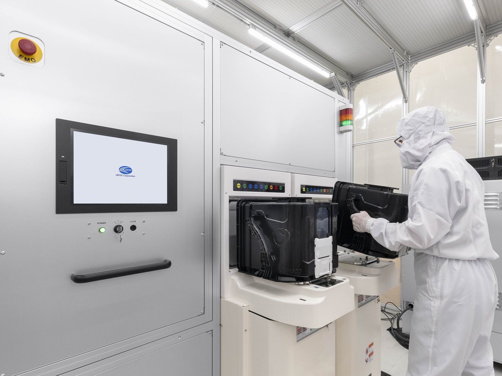
Equipment for mass producing Lintec CNT-based pellicle membranes
The contents of the News Release are as of the announcement date. Please note that they may differ from the latest information.