- HOME
- Topics
- News Release
- 2026
September 29, 2026
LINTEC to Expand Capacity for Semiconductor Equipment to Meet Growing Demand
New Building Constructed at Ina Technology Center
LINTEC has invested approximately 2.5 billion yen in the construction of a new building at its Ina Technology Center in Kita-Adachi District, Saitama Prefecture, a development and manufacturing base for various types of equipment. The new building will begin operations in October with the aim of enhancing the Company's capabilities for developing new equipment and further expanding its production capacity, with a particular focus on semiconductor-related equipment, demand for which continues to grow.
Four-Story Building to Begin Operations in October
Ina Technology Center serves as a development and manufacturing base for various types of equipment. These include systems for applying and removing specialized adhesive tapes used in semiconductor wafer back grinding (thinning) and dicing processes, as well as labeling machines that automatically apply labels to product packaging. Amid strong demand for semiconductors in recent years, production of semiconductor-related equipment has continued at close to the Center's current capacity limit. At the same time, sharp market fluctuations have made it necessary to fulfill orders with shorter lead times.
In response to these circumstances, LINTEC constructed a new four-story building at the Center. This expansion will increase the space available at the Center for the design, manufacture, evaluation, and testing of various types of equipment. The new building was completed on September 14 and will begin operations in October.
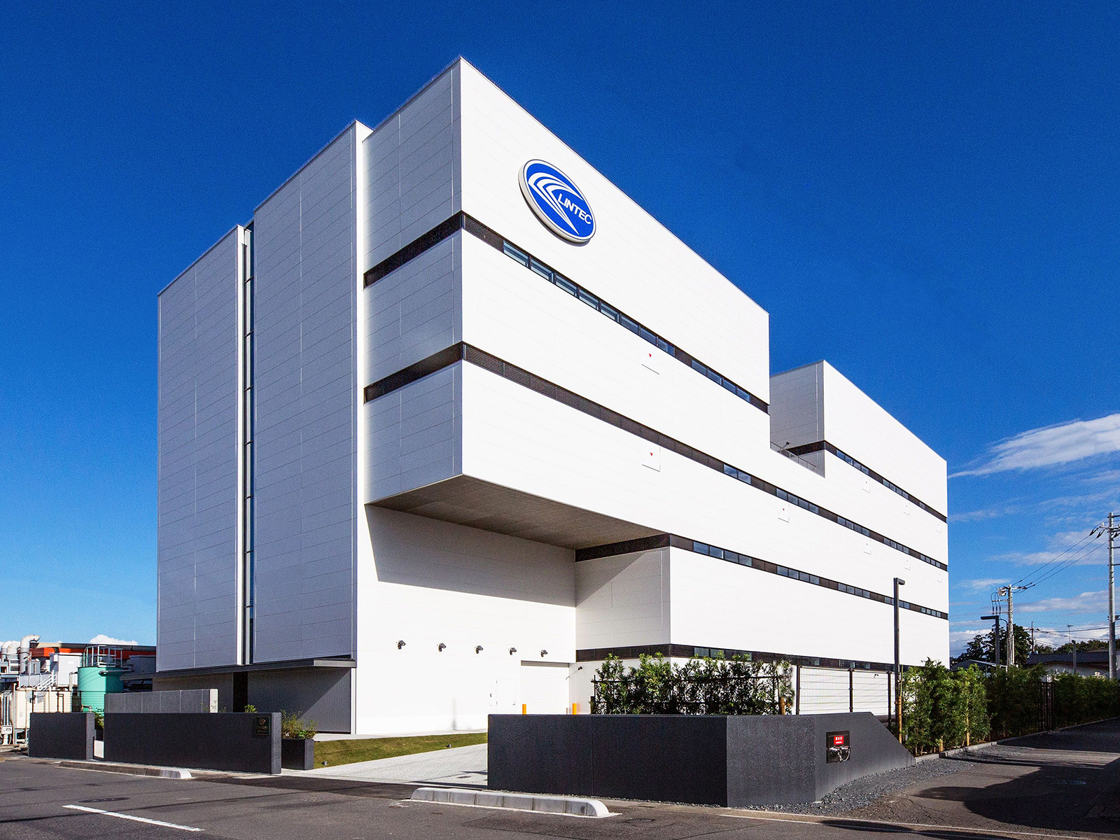
Exterior of the new building at the Ina Technology Center
Semiconductor Equipment Production Area Expanded 1.6-Fold
The new building will provide space for equipment design as well as for evaluating and testing equipment to customer specifications. These activities are currently carried out in the existing building. LINTEC will establish a dedicated development area with approximately 1.5 times the previous floor space, with the aim of strengthening its capabilities to develop new equipment in response to advances in semiconductor manufacturing technologies. All of the space freed up in the existing building will be allocated to manufacturing operations, resulting in substantial increases in floor space for both development and manufacturing. In particular, the area used for equipment assembly, adjustment, inspection, and other manufacturing processes will increase to approximately 1.6 times its current size, enabling LINTEC to expand production capacity in response to growing demand.
The new building is also equipped with solar panels to help reduce energy consumption and has been designed with accessibility in mind. LINTEC will continue to meet customer needs by providing comprehensive solutions that combine the tapes and equipment essential to semiconductor manufacturing processes.
Overview
- Ina Technology Center
- Location: Ina-machi, Kita-Adachi District, Saitama Prefecture
- Established: July 1983
- Employees: 308 (as of September 1, 2026; including temporary employees and employees of affiliated companies)
- New Building, Ina Technology Center
- Building area: Approx. 1,000m2
- Total floor area: Approx. 3,600m2
- Configuration: Four floors above ground
・First and second floors: Development areas (evaluation and testing of equipment in accordance with customer specifications)
・Third floor: Design area
・Fourth floor: Design area, meeting rooms, and other facilities
- Total construction cost: Approximately 2.5 billion yen
- Completion: September 2026
The contents of the News Release are as of the announcement date. Please note that they may differ from the latest information.