- HOME
- Topics
- News Release
- 2026
August 4, 2026
LINTEC to Open New Research Facility, “Semiconductor Solutions Lab,” in Fukuoka Prefecture, Japan
LINTEC has decided to open a new research facility, the Semiconductor Solutions Lab, on a site adjacent to the Fukuoka Solution Center for Advanced Semiconductor Packaging within the Itoshima Research Park (Itoshima City), an industrial research park in Fukuoka Prefecture. With a view to developing process materials, direct materials, and related equipment for mid-end semiconductor manufacturing processes, the facility is scheduled for completion in October 2028 with an investment of approximately ¥20 billion. The construction of the facility is also in line with the policies of Fukuoka Prefecture and Itoshima City to revitalize the local economy. Prior to construction, a three-party location agreement ceremony will take place on August 21 at the Fukuoka Prefectural Government Office.
Focusing on Technological Innovation: Strengthening Core Technologies from a Mid- to Long-Term Perspective
Demand for semiconductors―particularly for AI applications―continues to expand, driving a major turning point in semiconductor manufacturing technology. As devices become higher-performing and more densely integrated, the boundary between front-end and back-end processes is blurring. At the same time, technological innovations in mid-end processes, such as 3D integration and chiplet integration, are advancing, making these processes increasingly critical for performance, yield, and reliability.
LINTEC previously established the Package and Material Development Group as a dedicated research unit inside the Fukuoka Solution Center for Advanced Semiconductor Packaging, which is operated by the Fukuoka Industry, Science & Technology Foundation. On-site staff members have been driving the development of tapes, equipment, and processes for packaging technology. To build on these efforts and strengthen the company's technological foundation for mid- to long-term growth amid structural changes in the semiconductor industry, LINTEC decided to construct a new building on a site adjacent to the center to serve as a strategic development hub.
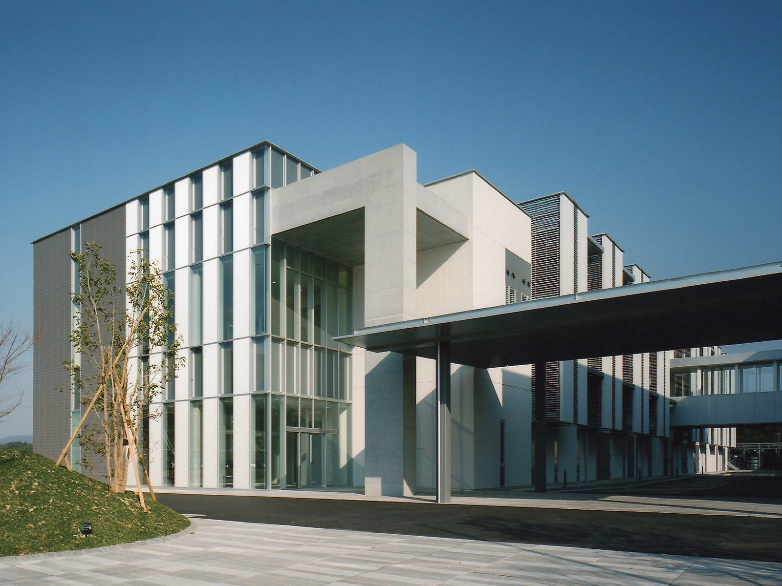
Fukuoka Solution Center for Advanced Semiconductor Packaging, where LINTEC maintains a presence
Responding Swiftly to Next-Generation Processes Through Co-Creation and Rapid Support for Customers
The newly established Semiconductor Solutions Lab will feature a clean environment equipped with various analytical and testing devices, as well as mid-end and back-end equipment manufactured by LINTEC and other vendors that runs on actual production lines. Positioned as a "co-creative and responsive" development hub where technological development is pursued hand-in-hand with customers, the facility aims to enable rapid adaptation to next-generation processes.
LINTEC operates Application Centers equipped with back-end equipment in Japan, Taiwan, Malaysia, and North America to propose optimal processing conditions (such as tape application and peeling), conduct material evaluations, and perform process verifications. The new research facility will also work closely with each Application Center to strengthen LINTEC's global R&D structure and enhance the group's overall capability to offer comprehensive proposals across materials, equipment, and processes.
Supplementary Materials
- Overview of Semiconductor Solutions Lab
- Total investment: Approx. 20 billion yen
- Scheduled completion: October 2028
- Location: Higashi, Itoshima-shi, Fukuoka Prefecture
- Site area: 3,435 m2
- Building: Three stories above ground, total floor area of approx. 5,000 m2
- Employees: Planned for approx. 25 (initially staffed by approx. 15)
- Research topics: Materials for semiconductor and electronic component manufacturing processes, etc.
- About LINTEC's Semiconductor-Related Business
- About the Fukuoka Solution Center for Advanced Semiconductor Packaging
LINTEC entered the semiconductor market in 1986 with the development of UV curable dicing tape. Today, it maintains a strong presence in the market for specialized pressure-sensitive adhesive tapes, primarily used in the back-end process of semiconductor manufacturing. A key strength of LINTEC's business in this sector is its ability to develop in-house not only adhesive tapes but also the specialized equipment required to apply and peel them.
Adhesive tapes are developed at the Research & Development Division and the Research Center (Warabi City and Saitama City, Saitama Prefecture), while equipment is developed at the Ina Technology Center (Kita-Adachi District, Saitama Prefecture).
Operated by the Fukuoka Industry, Science & Technology Foundation, this center was established in August 2025 through the integration of its predecessors: the Research Center for the Three-Dimensional Semiconductors and the Experimental Center for Social System Technologies. It serves as a comprehensive support hub covering everything from design and prototype development to evaluation, analysis, and verification testing leading to commercialization. The center is equipped with advanced equipment for high-density chip integration and packaging, including 3D stacking of multiple semiconductor chips.
In October 2023, LINTEC set up operations inside the predecessor Research Center for the Three-Dimensional Semiconductors and established its Package and Material Development Group. Since then, LINTEC has been driving the development of semiconductor-related products and new process technologies.
The contents of the News Release are as of the announcement date. Please note that they may differ from the latest information.