- HOME
- Topics
- News Release
- 2026
June 8, 2026
LINTEC Opens Advanced Development Center at Research Center
Strengthening Development of New Materials and Process Technologies for Advanced Semiconductors
LINTEC has opened the Advanced Development Center in its Research Center's Advanced Technology Building (Saitama-shi, Saitama Prefecture). The aim of this research facility, equipped with cleanrooms, is to strengthen the company's materials and process development system in the field of advanced semiconductors, including those for AI applications.
Evaluation Environment Closely Approximates Semiconductor Mass Production Line
As AI device performance has improved in recent years, chiplet technology is evolving in the field of advanced semiconductors, including High Bandwidth Memory (HBM) and logic devices. This technology integrates multiple chiplets into a single package through packaging and stacking. As chips become higher density and multi-die stacked, technologies such as hybrid bonding, which directly bonds chips without the use of adhesives, are also gaining in importance.
With direct bonding, however, even minor contamination and residue can significantly impact yield and reliability. For this reason, it is essential that materials and process technologies are properly managed and evaluated throughout chip manufacturing.
It is against this backdrop that LINTEC has invested a total of approximately 1.6 billion yen to establish its Advanced Development Center, which is equipped with ISO Class 5/Class 7 cleanroom environments. In addition to a variety of equipment developed by LINTEC, the Center houses mid- and back-end process equipment, including high-precision grinding, grooving laser*, and dicing equipment, as well as inspection equipment.
LINTEC is expanding and strengthening its capacity for evaluating materials and processes, including semiconductor-related tapes for HBM and other devices, for which low contamination and low residue are critical, under conditions that closely approximate those of mass production lines.
- *Grooving laser: Pre-processing equipment that uses a laser to form grooves prior to the dicing process
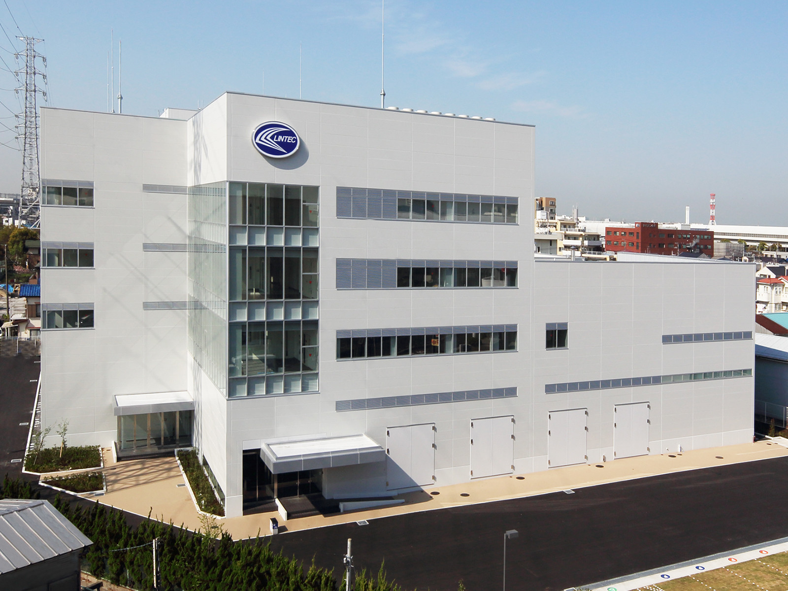
Exterior of Research Center's Advanced Technology Building
Strengthening Co-Creation to Offer Next-Generation Material and Process Solutions
LINTEC is engaged in developing new technologies through co-creation with external research institutions and companies. The development of materials and processes related to direct transfer bonding (DTB) is one such example. DTB is a process technology in which cut chips are temporarily laminated with tape for transport and alignment, allowing them to be placed on and bonded to a wafer with no direct contact with the chip surface. This process plays a crucial role in hybrid bonding by enabling high-precision chip mounting, while minimizing contamination.
LINTEC will utilize the Advanced Development Center as a hub for promoting collaborative research and development of this type. In addition to developing its own products, the company will strengthen its response to the rapid evolution of advanced semiconductor technology with the ability to conduct material evaluations and process verification in the presence of customers.
Overview
- Cleanroom Classification: ISO Class 5 / Class 7
- Floor Area: 158 m2 (total)
- Location: Research Center, Saitama-shi, Saitama Prefecture, Japan
The contents of the News Release are as of the announcement date. Please note that they may differ from the latest information.