- HOME
- Topics
- News Release
- 2026
February 18, 2026
LINTEC Develops Resin Coating Process for Flatter Semiconductor Wafers during Back Grinding
Accepting Full-Scale Orders for New RAD-3400F/12
LINTEC has developed Pattern Coating Before Lamination (PCBL), a process for the back grinding of semiconductor wafers that reduces thickness variation caused by step height differences on the circuit surface. The company will accept full-scale orders for the RAD-3400F/12, its new resin coater for eliminating step height differences, from April 2026.
PCBL Process Reduces Uneven Wafer Thickness
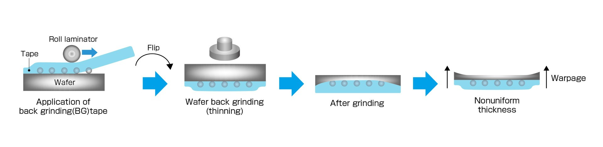
As semiconductor chips are increasingly miniaturized, the process of back grinding wafers to reduce thickness and achieve flatness has become more and more important to the manufacturing industry. In particular, the ability to suppress thickness variation across the wafer and ensure a flatter surface is especially crucial to improve the quality of semiconductor chips. However, differences in thickness between the center and outer edges, as with wafers on which protruding electrodes, called bumps, are formed on the circuit surface, create uneven thickness along the outer edge when back grinding tape is applied to protect the surface during wafer grinding. This difference can also cause cracks to form during the grinding process.
To resolve this issue, LINTEC developed its new PCBL process, which eliminates step height differences by coating the bump-free outer periphery with UV curable resin, thereby resolving variations in thickness and reducing cracking.
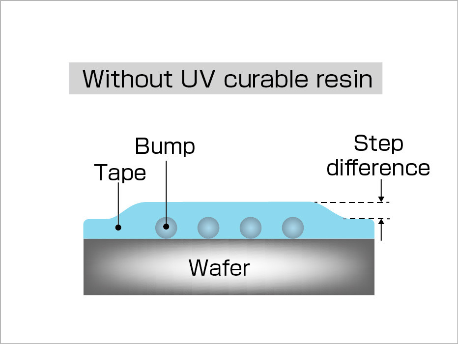
Cross-section of bumped wafer with back grinding tape applied
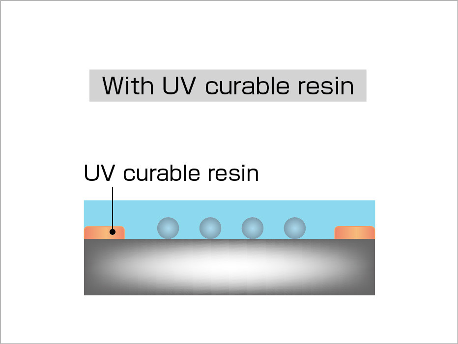
Cross-section of bumped wafer with back grinding tape applied (With UV curable resin)
RAD-3400F/12 Matches Resin Coating to Specifications
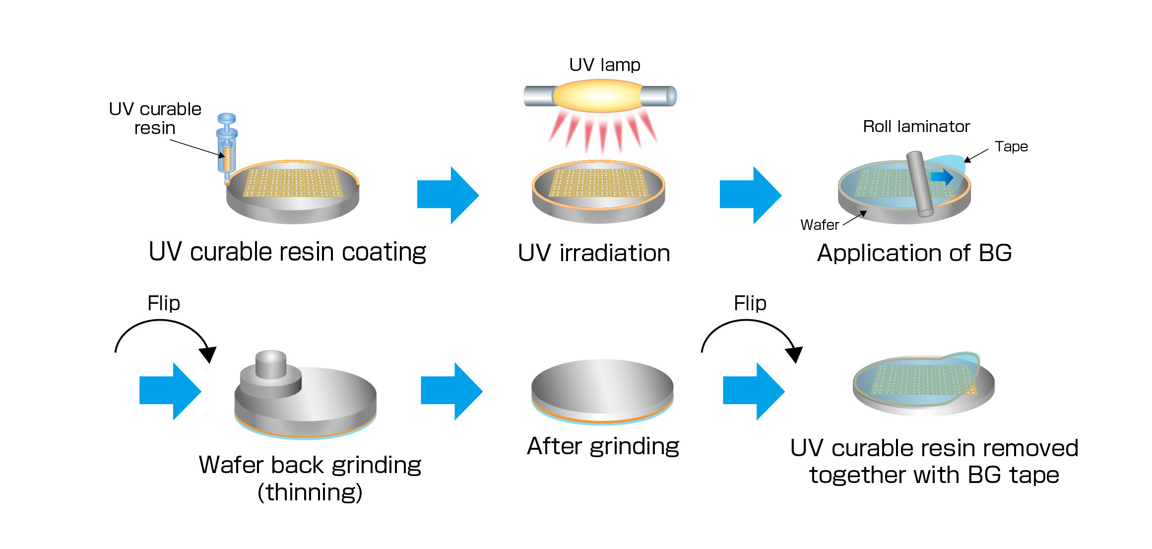
LINTEC developed the RAD-3400F/12 for the application of a coating of resin to wafers during the pattern coating process. The coater allows the resin pattern to be adjusted, making it possible to customize the amount, width, and height of resin application to match bump height and other wafer specifications. Once the resin is applied, conventional production lines can be used to apply back grinding tape for back grinding. When grinding is complete, the resin can be removed together with the back grinding tape.
By enhancing its solution through the coater and PCBL process, LINTEC aims to further contribute to improving yields in semiconductor chip manufacturing.
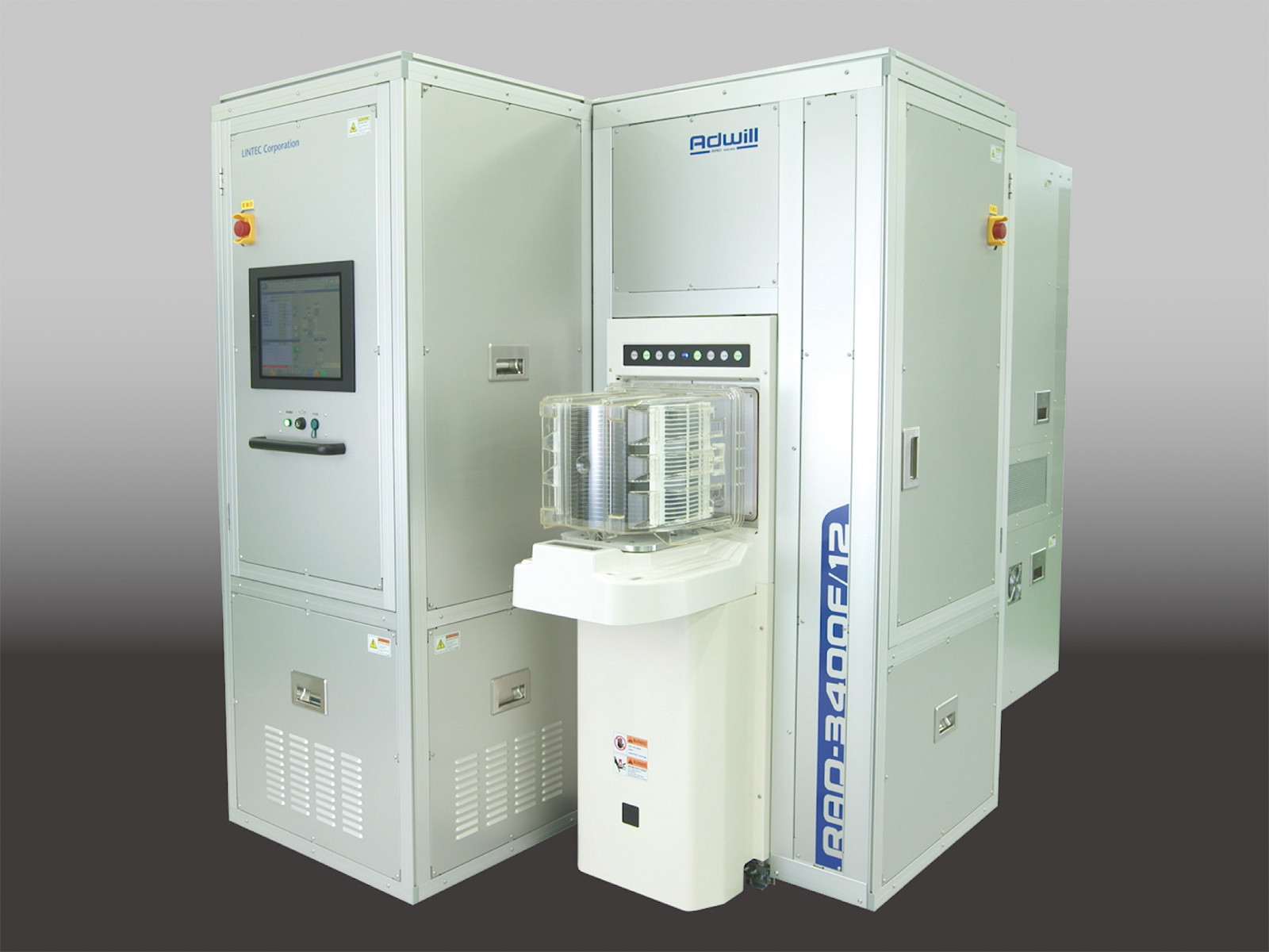
RAD-3400F/12
Product/Process Overview
- Characteristics
- The PCBL process is designed to resolve differences in thickness and reduce cracking during the semiconductor wafer back grinding process, which are caused by variations in thickness between the center and outer edges of wafers.
- The company's newly developed RAD-3400F/12 coater applies resin to semiconductor wafers. The coater eliminates uneven thickness that occurs when back grinding tape is applied by coating thinner areas of the circuit surface with UV curable resin.
- The RAD-3400F/12 enables customization to match bump height and other wafer specifications by adjusting the coating pattern, amount, width, and height. Once the resin is applied, conventional production lines can be used to apply back grinding tape for back grinding. When grinding is complete, the resin can be removed together with the back grinding tape.
- The RAD-3400F/12 can be integrated in line with the LINTEC back grinding tape application system RAD-3520F/12, enabling a new process to be added into existing production lines without the need for line modification.
- Back Grinding and PCBL Processes
Image of variation in thickness in back grinding process (cross-section)
PCBL process for UV curable resin coating
- On sale from April 1, 2026
The contents of the News Release are as of the announcement date. Please note that they may differ from the latest information.