- HOME
- Topics
- News Release
- 2017
April 28, 2017
New model of semiconductor-related system with high functionality and small-footprint
Back Grinding Tape Laminator “RAD-3520F/12”
Improved performance in anticipation of new semiconductor demand for cutting-edge devices and IoT
LINTEC develops and provides a tape laminator to protect the circuit surface of the wafer during the back grinding and thinning process of the semiconductor wafer after circuit formation. We have now improved the performance of the top-selling model “RAD-3510F/12” and have developed the “RAD-3520F/12,” which offers better performance and a smaller footprint. It will be launched on May 1.
Next-generation back grinding tape laminator
Along with the evolution of electronic devices and the development of the Internet of Things (IoT) market where everything is connected to the Internet, their core parts, semiconductor chips are becoming smaller and more dense. In addition, semiconductor manufacturing systems are now required to have the ability to handle both ultra-thin wafers and wafers with bumps (protruding electrodes on the circuitry) used in the Wafer Level Package (WLP)*1 technology, demand for which is growing.
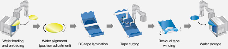
Our “RAD-3510F/12” is a system that laminates tapes for protecting the circuit sides of wafers during back grinding or thinning process of wafers after circuits are formed on them. It reduces the risk of damage during in-line wafer transport and is capable of handling both wafers with bumps and ultra-thin wafers. This system has achieved an excellent reputation in the market. We have now redesigned the laminator and have further improved its performance and production capacity.

Further improved productivity and enhanced optional features
The “RAD-3520F/12,” a new back grinding tape laminator, has reduced its footprint by approximately 30% compared to conventional models in order to satisfy the downsizing requirements. Despite the downsizing, it is still equipped with two wafer loading units called load ports and achieves outstanding production capacity. Its wafer processing ability has improved by up to 66% (improved from 60 wafers per hour to 70 wafers per hour; up to 100 wafers per hour as an option).
Furthermore, the number of processed wafers per roll of tape (total length: 100 m) has increased by up to 16% by shortening the tape cut pitch.*2 Various cleaning functions and diverse options, which contribute to labor saving including cutter replacement and tape replenishment, are available to meet customer needs. As with conventional models, this laminator is also equipped with a unique tape tension control mechanism*3 and a multi-joint robot arm, which is used for wafer handling and tape cutting. This multi-joint robot arm enables a high-precision cutting profile with accurate control of the cutter angle, which helps to solve problems during back grinding caused by the cutting burr of the tape.
- *1WLP (Wafer Level Package): A technology that performs package processing up to the final process, from rewiring to electrode formation, resin sealing, and wafer separation at the wafer level. Compared to general packaging methods, this technology is suited for downsizing and weight reduction of packages.
- *2When the wafer diameter is 300 mm (12 inch).
- *3Tape tension control mechanism: A mechanism that is capable of high precision tension control during the tape lamination to prevent warpage of and damage to ultra-thin wafers.
Operation process
Specifications
- Equipment size: 1,245 mm (W) × 1,850 mm (D) × 1,890 mm (H) *Excluding the signal tower
- Applicable wafer size: 200 mm (8 inch), 300 mm (12 inch)
The contents of the News Release are as of the announcement date. Please note that they may differ from the latest information.